PCB Material
Why partner with COFAN-USA?
- 1. Technology
- 2. Quality
- 3. Responsiveness
- 4. Delivery
- 5. Cost
- Promotion
- View detail >>
SMTA & Final Assembly(OEM)
With our strength of MCPCB, heat sink, assembly and full function design capabilities,
we can provide a one...
> view more
we can provide a one...
> view more
- Contact us
- Go to
contact us >>
- Price Quote
- Go to quote >>
All your quality products supplier.
MCPCB
Home > Products > MCPCB
Overview
- Single Layer, Multiple Layer MCPCB or FR4
- Surface mounted components / wave soldering
- Solder mask coloring
- Machined features
- Low / High volume
- Turn key operation
- Quick lead time / turn around
- Testing
- Cables / Connectors
Applications
MCPCB Benefits
- Components operate at lower temperatures
- Durable
- Flatness maintained in all 3 layers
- High Heat Dissipation
- High density of components
- Reduced PCB size / Small footprint
- Higher Watt Density
- Longer component life
- Less hardware (topical heat sinks, screws, clips, etc)
- Lower Manufacturing Cost
Services We Offer
- Excellent customer service
- Low-cost
- Rapid prototyping
- Complete thermal analysis / design
- Custom heat sinks
- Mechanical design
- Circuit / Electrical design
Service and Leadtimes
- Prototype
- 1-4 panels
- 3 days, 5 days and 7 days quick turns
- 7 days standard delivery
- 18"x 24"panel size
- Production
- 4 + panels
- 2 weeks standard delivery
- KANBAN or Stocking programs available
- Multiple panel sizes
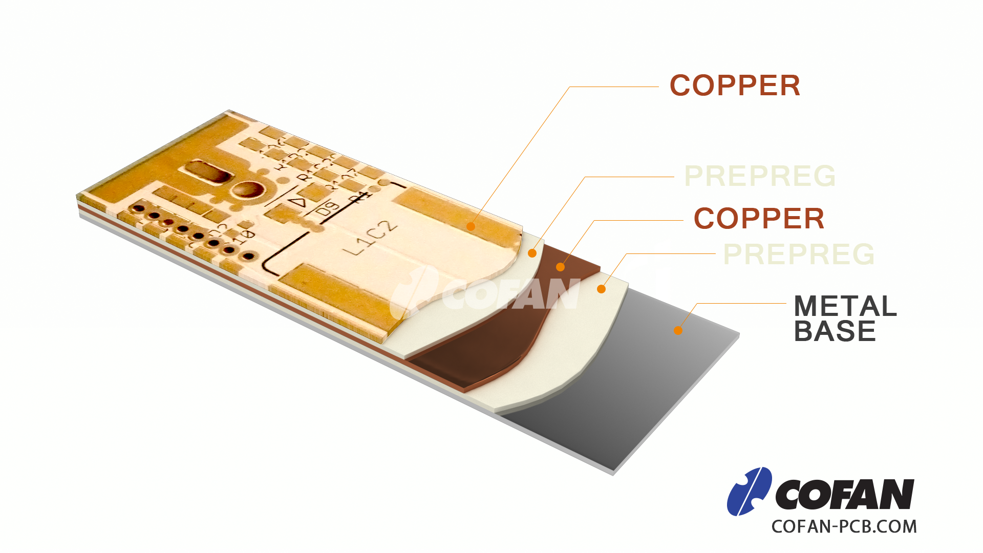
- Material of MCPCB
For more information
Thermo Conductive Pillar for Modular LED Array
Out of over 50 projects we have done in the past, Cofan obatained 16 patents for MCPCB technology. This is an example of how we work in order to achieve the best quality products from Cofan. We know exactly what MCPCB technology is and this experiment is not the end and we will continue to create better solutions for the market in the future.
What technological advancements were we trying to achieve?
The technological objective of this project was to develop a new LED module for high luminous efficacy.
The technological objective of this project was to develop a new LED module for high luminous efficacy.
Historically, the state of the art in MCPCB based LED technology consisted of a metal core base layer, covered with a dielectric layer (where the circuit is formed). Wires re manually soldered to the traces to achieve operational conductivity. The thermal conductive pillar for the LED modular array will improve efficiency and cross-platform design. With the current technology resistance arcing acts a limiting factor as high current LED drivers require 1500V (3 second interval). The dielectric layer limits the circuit due to the barrier it creates between the two layers establishing a thermal conductivity of 200W/K*m. Additionally, significant portions of light is typically reflected by the surface of the waveguide and is absorbed and scattered by substrate as the dielectric layer, the electrode pads and wires covering the substrate have very low reflectivity limiting the luminous efficiency to 60 Lumens/W.
To overcome these constraints, Cofan sought to develop the following:
- New thermal management technologies in Metal Core Printed Circuit Board (MCPCB) capable of achieving a conductivity of 320 W/m-K. This new module technology would withstand a 1500V exposure for a period of 3 seconds.
- New thermal management technologies in Metal Core Printed Circuit Board (MCPCB) capable of achieving a conductivity of 320 W/m-K. This new module technology would withstand a 1500V exposure for a period of 3 seconds.
- Integrate the new LED module with top reflective surface layer with a waveguide structure to improve luminous efficiency to 90 Lumens/W wit new technology to combine metal core technology with an aluminum reflective panel.
However, this proved to be challenging as increasing the conductivity required the removal of burr induced conducing tracts formed through the mechanical forces present through drilling. For this reason Cofan needed to redevelop a method to form the necessary etched cavities. Additionally, Cofan encountered challenged in the new module with the top reflective surface as Cofan was uncertain of the optimal bonding procedure involving the pre-impregnated glass fiber material with two sandwiching layers, total of three layers, as Cofan had never bonded more than two layers.
If successful, this technology could be applied to light-emitting diodes (LED) lighting mounted on a surface module, maintaining high thermal conductivity while performing in a high current driver application. Cofan seeks to develop a module that can essentially be handled as a plug-and-play LED device while increasing the lumen output the overall efficiency and applicability increase drastically.
Through this project Cofan advanced their scientific knowledge in the field of electrical engineering by developing a LED module to improve the thermal conductivity, luminous efficiency and the technology of the MCPCB to effectively withstanding a 1500V exposure for 3 second duration and sought to improve luminous efficacy to upwards of 90+Lumens/W.
What technological obstacles did we have to overcome?
The technological obstacles encountered in the fiscal year, revolved around developing a high current driver, high luminous efficacy LED module combining new Metal Core PCB heat dissipationo technologies with a new aluminum reflective panel integrated with the Metal Core PCB.
The technological obstacles encountered in the fiscal year, revolved around developing a high current driver, high luminous efficacy LED module combining new Metal Core PCB heat dissipationo technologies with a new aluminum reflective panel integrated with the Metal Core PCB.
Specifically, Cofan encountered the following technological obstacles in the fiscal year:
Dielectric strength (resistance to arcing) and consistency of epoxy flow
- Cofan needed to alter the drilling process when forming small cavities intended for current insulation to prevent the formation of undesirables conducting tracts. Initial attempts of using a drilling process resulted in the development of copper burrs which essentially created conducting tracts, which compromised dielectric strength; due to the substantial mechanical forces and over-stressing yields displaced on the copper plating which was present during this operation.
- Cofan needed to alter the drilling process when forming small cavities intended for current insulation to prevent the formation of undesirables conducting tracts. Initial attempts of using a drilling process resulted in the development of copper burrs which essentially created conducting tracts, which compromised dielectric strength; due to the substantial mechanical forces and over-stressing yields displaced on the copper plating which was present during this operation.
Voids in the substrate layer and lamination impacts
- Cofan needed to establish a correlation between the change in Cu and the PCB edge distance relative to the BDV in the air, to actively prevent the failures due to voids in the non-conductive epoxy resin. Initial attempts using a chemical etching process resulted in the formation of unpredictable voids forming within the epoxy which decreased the dielectric strength significantly.
- Cofan needed to establish a correlation between the change in Cu and the PCB edge distance relative to the BDV in the air, to actively prevent the failures due to voids in the non-conductive epoxy resin. Initial attempts using a chemical etching process resulted in the formation of unpredictable voids forming within the epoxy which decreased the dielectric strength significantly.
Optimal cavit profile for epoxy resin flow
- Cofan was uncertain of the optimal size and shape of the cavities required to allow for consistent resin flow to minimize voiding. As such, experimentation with various pocket sizes within the cavity was required to allow for consistent resin flow to minimize voiding. As such, experimentation with various pocket sizes within the cavity was required to improve the initial flow of the epoxy resin and thereby preventing formation of voids and air bubbles. The initial cavity pocket size of 0.109” failed to allow the epoxy to initially flow into the barrel and prevent voids.
- Cofan was uncertain of the optimal size and shape of the cavities required to allow for consistent resin flow to minimize voiding. As such, experimentation with various pocket sizes within the cavity was required to allow for consistent resin flow to minimize voiding. As such, experimentation with various pocket sizes within the cavity was required to improve the initial flow of the epoxy resin and thereby preventing formation of voids and air bubbles. The initial cavity pocket size of 0.109” failed to allow the epoxy to initially flow into the barrel and prevent voids.
LED reflective panel to improve luminous efficacy
- Cofan was uncertain how the mechanical processes to form the reflective panel and the distortions in the panel would impact the laminate adhesion as well as the overall luminous efficacy of the assembled module. Initial attempts using the reflective panel resulted in yield rates below 50% due to leakage of pre-impregnated glass fiber material into the LED pocket, resulting in contamination.
- Cofan was uncertain how the mechanical processes to form the reflective panel and the distortions in the panel would impact the laminate adhesion as well as the overall luminous efficacy of the assembled module. Initial attempts using the reflective panel resulted in yield rates below 50% due to leakage of pre-impregnated glass fiber material into the LED pocket, resulting in contamination.
What work did we perform in last year to overcome those technological obstacles?
Dielectric strength (resistance o arcing) and consistency of epoxy flow
Initially Cofan theorized, utilizing a drilling process to maintain material properties by avoiding substantial mechanical forces and stresses preventing the formation unwanted conductor tracts. To do so Cofan experimented by drilling small cavity hole for the current insulation on the copper trace. However, with this process, Cofan observed that there was a strong presence of copper burs which compromised the dielectric strength resulting in the circuit unable to withstand resistive arcing at/exceeding 1500V for the duration of 3 seconds. In attempts to resolve this issue and inherently minimize the probability of resistance arcing, Cofan hypothesized that a chemical process would reduce the level of induced stress and deformation (through a cold process) in order to maintain the original properties while preventing the formation of burs. A hydrochloric acid and copper sulphate based formulation was experimented with as an etching solution; the chemical was intended to remove the copper silvers quickly to ensure no damage occurs to the copper base. Testing this theory Cofan immersed the copper board into the solution. Cofan observed a buildup of cupric chloride, where the disproportional reaction took over cuprous chloride. With this strategy, Cofan observed improved consistency with the high-pot tests.
Voids in the substrate layer and lamination impacts
However, with this new etching strategy Cofan also observed higher failure rates as unpredictable voids began to form on the epoxy resin, compromising the dielectric strength of the trace. Cofan performed further testing to develop a correlation between the change in Cu and he PCB edge distance relative to the BDV in the air, bounding the distance between 1mm-5mm. A series of 6 distances with 1mm increments and 1.5mm were tested, analysis of the results showed that distance between the Cu and PCB edge relative to the BDV (kV) had a linear correlation exhibiting potential optimal distances for curing of the epoxy based on a resin thickness of 200VDC/mm.
However, with this new etching strategy Cofan also observed higher failure rates as unpredictable voids began to form on the epoxy resin, compromising the dielectric strength of the trace. Cofan performed further testing to develop a correlation between the change in Cu and he PCB edge distance relative to the BDV in the air, bounding the distance between 1mm-5mm. A series of 6 distances with 1mm increments and 1.5mm were tested, analysis of the results showed that distance between the Cu and PCB edge relative to the BDV (kV) had a linear correlation exhibiting potential optimal distances for curing of the epoxy based on a resin thickness of 200VDC/mm.
Through further experimentation Cofan identified the difficulty was arising due to the application process of the non-conductive epoxy into the insulation cavity as it contained a copper base contamination. Cofan observed the cavity barrels were too deep to avoid the air trap at a base thickness of 0.125”. To overcome this team experimented by securing the epoxy inside the barrel and implementing a vacuum bed effectively descend the epoxy resin to the base, during the screening process. Experimentations showed improvements in yield however, results were still considered poor as the failure rate was measured to be 25% alongside a lack of consistency. Upon further inspection Cofan was able to correlate the failure to the high degree of viscosity of the epoxy.
To resolve this, Cofan experimented with the use of pre-treatment methods which enhanced the lamination by forming an oxide layer, increasing bond strength within the copper base, Using black oxide Cofan converted the surface of the material to magnetite(Fe3O4) which offered sufficient corrosion resistance. Testing this pre-treatment Cofan applied oxide layer on a single side of the copper base. Cofan performed a sequential process comprising of pre-clean,, water rinse, micro-etching, water rinse, black oxidation process, water rinse and finally a 60 degree baking process. Cofan experienced positive results as the pre-treatment increased the bond strength to an optimal degree, however, the epoxy still continued to form voids.
Optimal cavity profile for epoxy resin flow
Cofan hypothesized that by altering the pocket shape of the cavity; this would improve the initial flow for the epoxy resin and prevent the voiding defects. This was to be achieved by increasing the distance between the electrode’s hole and base. Testing this theory Cofan experimented with two types of cavity, a conical countersink and a larger cylindrical. Cofan found the larger cylindrical barrel opening to work more optimally in comparison to the conical countersink as the larger opening allowed the epoxy to flow more consistently due to the higher viscosity.
Cofan hypothesized that by altering the pocket shape of the cavity; this would improve the initial flow for the epoxy resin and prevent the voiding defects. This was to be achieved by increasing the distance between the electrode’s hole and base. Testing this theory Cofan experimented with two types of cavity, a conical countersink and a larger cylindrical. Cofan found the larger cylindrical barrel opening to work more optimally in comparison to the conical countersink as the larger opening allowed the epoxy to flow more consistently due to the higher viscosity.
LED reflective panel to improve luminous efficacy
In parallel, Cofan attempted to develop a top reflective surface layer with a waveguide structure to increase the luminous efficacy. Cofan hypothesized that by dividing the pre-impregnated glass fiber material into two sections with varying curing stages, half cured (B stage) and fully cured(C stage), this would eliminate resin starvation when bonding to a third surface. Testing this theory Cofan experimented with different section thickness and cure stages to achieve the optimal lamination strength with the metal core layer. Through experimentation Cofan observed optimally a layer of thickness 0.006” required two 0.003” sections in which the fiber material attached to the copper foil is in the C stage and the other section in B stage is layered above it prior to the mechanical punching(to form the pocket). Following this Cofan interlaid the aluminum reflective panel and pressed both components together without resin starvation resulting in delaminating. However, during the pressing process Cofan observed resin flowing into and contaminating the LED cavity.
In parallel, Cofan attempted to develop a top reflective surface layer with a waveguide structure to increase the luminous efficacy. Cofan hypothesized that by dividing the pre-impregnated glass fiber material into two sections with varying curing stages, half cured (B stage) and fully cured(C stage), this would eliminate resin starvation when bonding to a third surface. Testing this theory Cofan experimented with different section thickness and cure stages to achieve the optimal lamination strength with the metal core layer. Through experimentation Cofan observed optimally a layer of thickness 0.006” required two 0.003” sections in which the fiber material attached to the copper foil is in the C stage and the other section in B stage is layered above it prior to the mechanical punching(to form the pocket). Following this Cofan interlaid the aluminum reflective panel and pressed both components together without resin starvation resulting in delaminating. However, during the pressing process Cofan observed resin flowing into and contaminating the LED cavity.
Cofan theorized modifying the resin placement further from the cavity to account for the resin flow characteristics. Testing this theory Cofan studied the flow characteristics within the pre-impregnated layer and systematically determined a layer offset positioning of 0.002” from the pocket should be established to prevent flow run off and contamination sourced defects.
At the end of the fiscal year, Cofan was able to achieve a prototype capable of 85 Lumens/W with the combination of the technologies, however did not meet their overall target of 90+Lumens/W. Cofan has not been able to achieve acceptable consistency in adhering the reflective panels to the MCPCB. Additionally Cofan encountered a yield rate of 50%due to excessive positional tolerance offsets. Cofan plans to continue this project in the future. Cofan plans to continue work in the next fiscal year.
 LinkedIn
 Facebook
 YouTube
 Google +